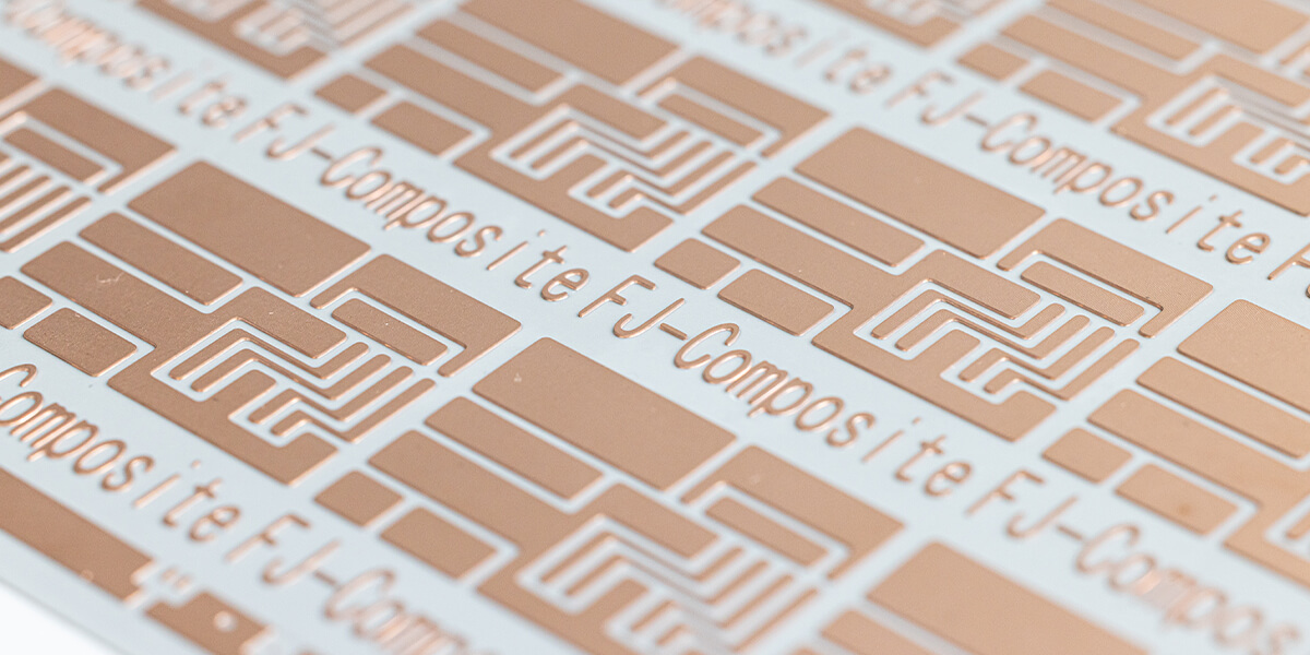
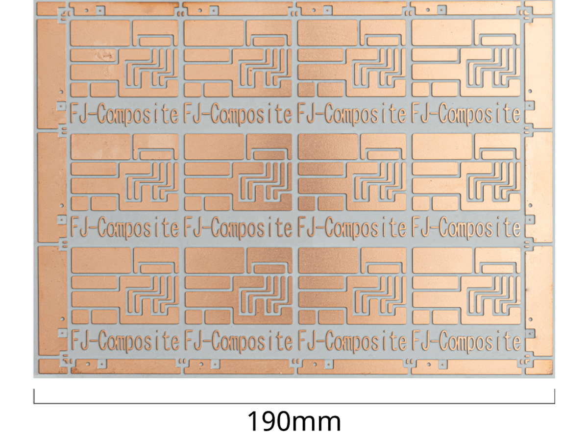
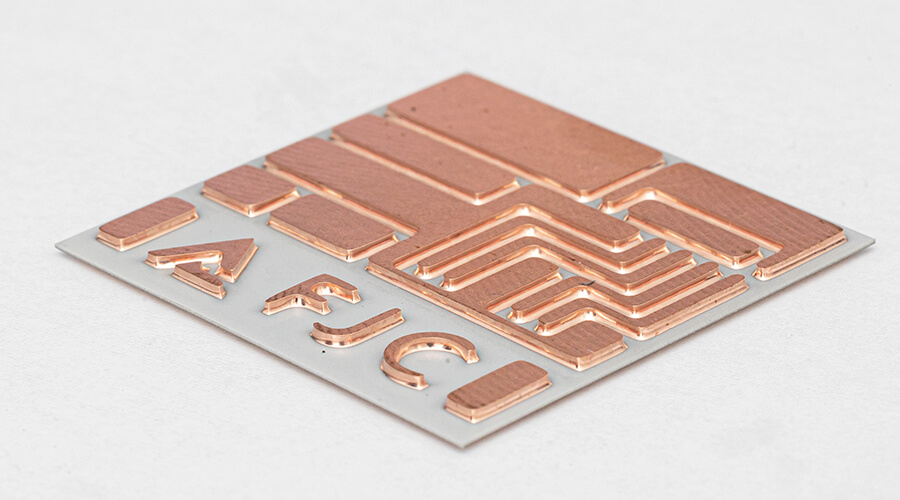
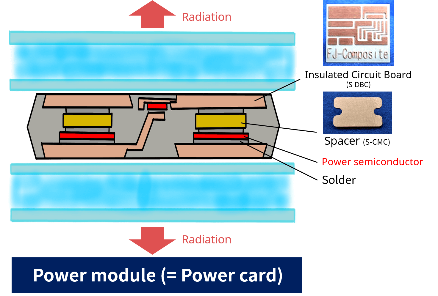
S-DBC
S-DBC is an ideal ceramic insulated circuit board with no voids. In high temperature conditions, large power electric devices can sometimes have issues, making thermal design and heat dissipation critical.
Our S-DBC offers high heat dissipation and bonding strength, making it a valuable addition to power modules operating in harsh environments.
Materials and Structures
Laminated structure of copper and ceramics (Si3N4, AlN, BeO, , Al2O3)
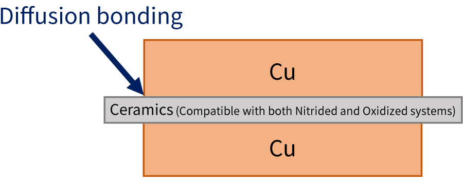
S-DBC by means of our original sputtering and diffusion bonding method
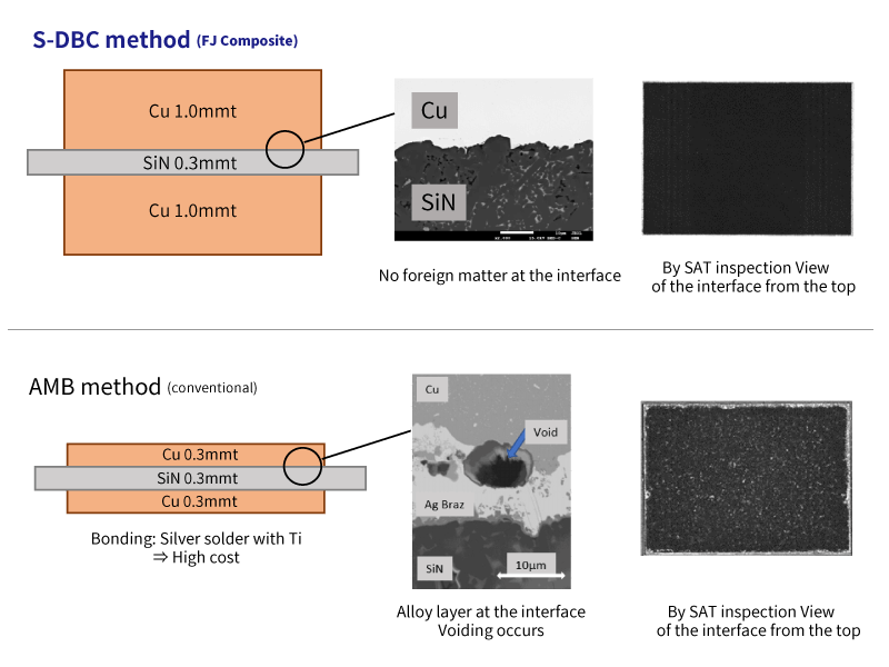
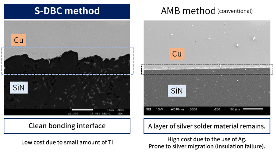
The alloy layer at the bonding interface of our S-DBC products is very thin and has no voids.
Therefore, it has higher performance (heat dissipation and bonding strength) than conventional DBC (Direct Bonding Copper) and AMB (Active Metal Bonding) methods.
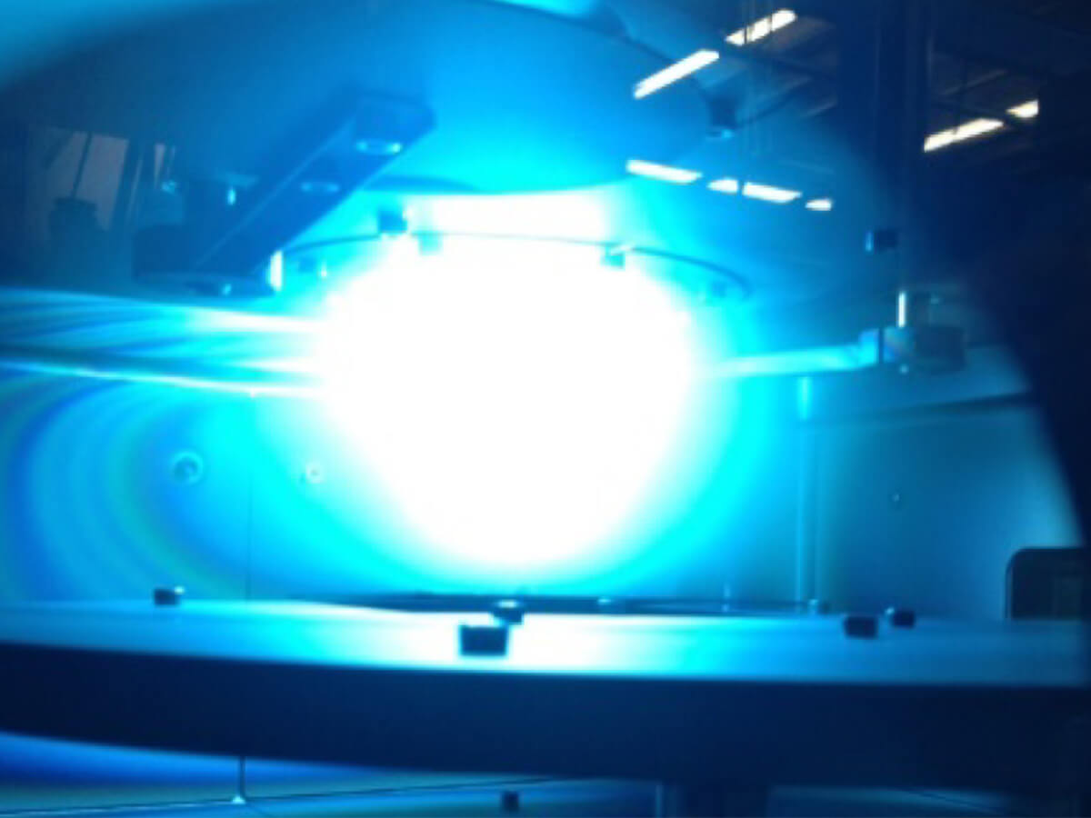
(1)Sputtering
(Ti deposition process)
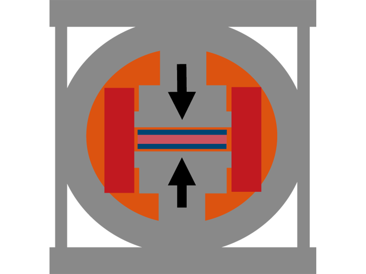
(2)Hot pressing
(copper plate bonding)
(3)Etching process
(circuit formation)
Physical Properties
Performance
Higher bonding strength
Peel test(50mm/min)
| Cu 0.3mmt | 15 N/mm |
|---|---|
| Cu 0.8mmt | 35 N/mm |
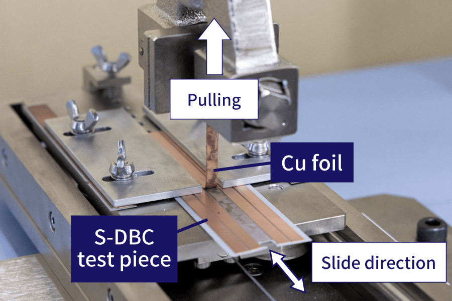
The state of the peel test
Bonding interface between copper and ceramics with no voids
There is only a very thin sputtering layer, and no voids were detected during the SAT analysis.
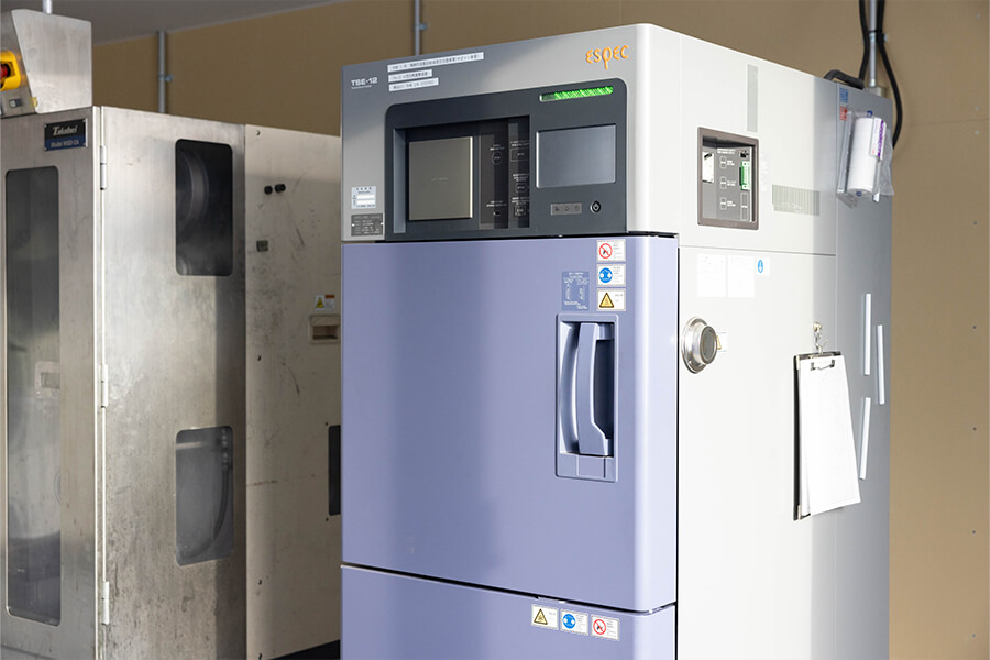
Reliability test
①Thermal shock test
(-50~150℃/cycle, dwell time15min, @each Temp)
| -55~150℃/5000 times | Passed by one user |
②Observation results of the bonding interface of DBC substrates
| -40~250°/3000 times | Passed by the national institute of advanced industrial science and technology |
Shape Processing and Manufacturing
(Diffusion bonding by hot press furnace)
Copper with thickness of 1mm or more can be formed.
High-precision thickness control
With our S-DBC method, it is possible to adjust the thickness of Cu in units of 10 μm.
Asymmetric layering of copper is also possible
High flatness/smoothness
The conventional method (AMB) had a thickness tolerance of about ±50 μm due to the alloy layer at the interface of Cu and ceramics, which was not uniform.
Our S-DBC method can be managed with a thickness tolerance of ±10 μm.
Processing image of thick copper T=1mm
Comparison with Conventional Manufacturing Methods
Conventional method 1: DBC(Direct Bonding Copper)
A lamination pattern is limited to Cu and oxide-based ceramics.
Conventional method 2: AMB (Active Metal Bonding)
A lamination pattern is limited to Cu and nitride-based ceramics.
FJC: S-DBC method(Sputtering Diffusion Bonding Copper)
Both oxide-based and nitride-based ceramics are applicable.
The bonding method is achieved through uniform Ti deposition by sputtering and solid-state diffusion bonding. Since the Ti layer is very thin, it has high thermal conductivity and bonding strength. In addition, cost reduction through large-area bonding is also possible.
Cost Performance
Low cost because rare materials are not used
Unlike the conventional AMB method, no silver solder is used, so there is no occurrence of silver migration (insulation failure).
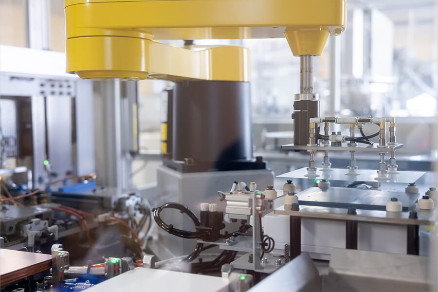
High productivity
Large size materials can be processed by the hot press furnace.
Suitable for mass production
We have established our own manufacturing method and production line.
[For mass production]
We have established and operated a mass production system from material preparation to molding, which can produce large quantities with minimal energy.
[For prototyping through customization]
We can provide a prototype at a low cost thanks to our unique production method.
Technology Solutions
Electric Vehicle Power Control Unit (PCU)
Electric vehicles can efficiently convert DC to AC and AC to DC very frequently.
The control device in electric vehicles, called the electric power control unit (PCU), consists of several power semiconductors that make it highly efficient.
During acceleration, the PCU converts the battery’s electric power from DC to AC and supplies power to a motor, as an AC control system is more advantageous.
During deceleration, it converts electric power from AC to DC to recover regenerated electric power.
S-DBC as an insulated circuit board in double-sided cooling power devices
The main devices that support a high-power system are called power modules, and they typically consist of ceramic insulating circuit boards. These circuit boards are made by bonding semiconductors (such as silicon/Si and silicon carbide/SiC) and various parts to a copper circuit that is formed on ceramics.
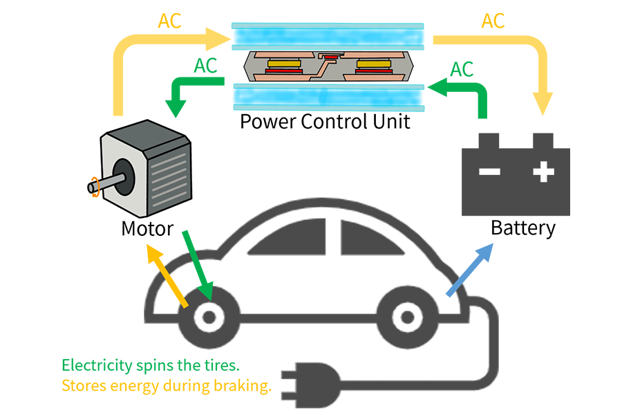
Mechanism of an Electric Car
During acceleration: the motor runs through the PCU via the battery.
During deceleration: the power generated by the brakes is stored in the battery via the PCU.
Structure of PCU
IGBT (high-power frequency conversion device)
IGBT is a type of power semiconductor used in high-power frequency converters, known for its high-speed switching capability. Some examples of high-power systems that use IGBTs include bullet trains, solar power generators, inverters, and industrial air conditioners.
As more information is processed and more semiconductors are stacked, more heat is generated. To address this, S-DBC is a ceramic insulating circuit board designed to effectively dissipate heat and withstand harsh environmental conditions.
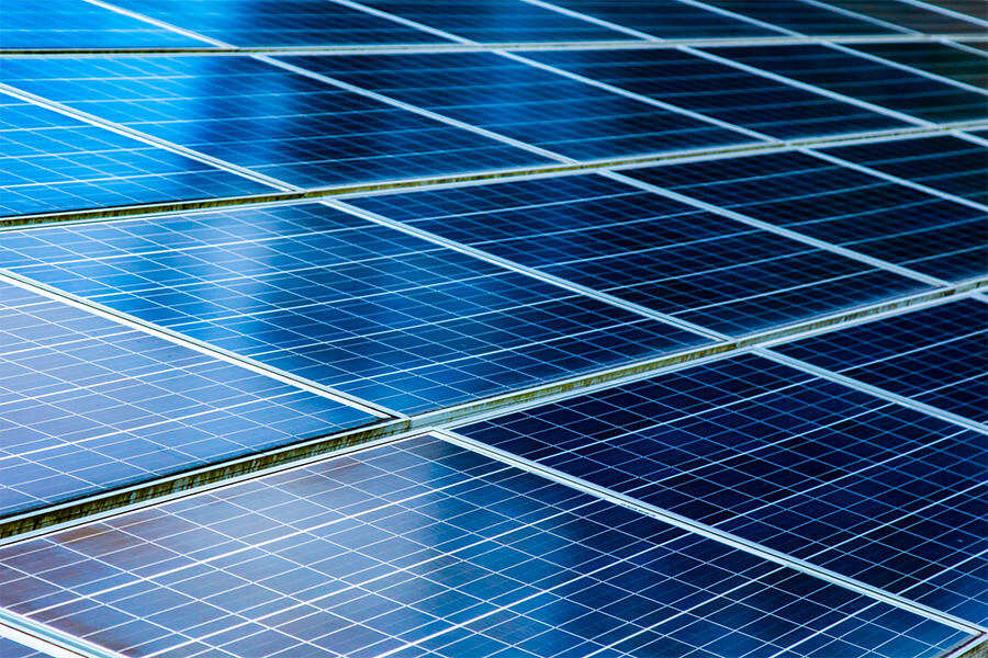
Used in shinkansen (bullet trains), solar power generation, and more
Awards
- Nominated for AIST’s Technical Support Achievements
- Newspaper feature
- Small and medium-sized enterprise foundation technology advancement (ceramic insulated circuit board) [Ministry of Economy, Trade, and Industry]
- Exhibited at Go Tech
- Nominated for Regional future driving company [Ministry of Economy, Trade, and Industry]